The Internet of Things (IoT) is expanding rapidly across every global industry. This massive growth demands autonomous, decentralized power sources for smart sensors, wearables, and remote monitors. We can no longer rely solely on standard power grids or disposable batteries to keep billions of devices online.
Manufacturing micro-solar panels for these modern devices poses a unique production challenge. You must cut standard solar cells into miniature, highly customized shapes to fit unique device casings. If done incorrectly, this cutting process induces micro-cracks and causes severe efficiency degradation. Moving away from utility-scale module production toward high-precision IoT component manufacturing requires specialized, non-contact tooling.
This article equips production managers and procurement engineers with an evidence-based evaluation framework. You will learn how to assess precision cutting equipment effectively. We provide actionable insights to help you scale IoT solar cell production efficiently, eliminate scrap, and protect your long-term profit margins.
Key Takeaways
IoT devices demand custom-sized, highly efficient micro-solar cells, rendering traditional mechanical cutting obsolete due to high scrap rates and edge degradation.
A high-precision Laser Scribing Machine minimizes the Heat-Affected Zone (HAZ), preserving the electrical integrity required for low-light IoT applications.
Evaluating a Laser Solar Cell Cutting Machine requires looking beyond base speed, prioritizing beam quality, automation integration, and vendor-supported Proof of Concept (PoC) testing.
The Business Problem: Why IoT Demands Rethinking Solar Cell Cutting
The standards for solar component manufacturing have shifted dramatically. Unlike standard 60 or 72-cell utility modules, IoT solar components face entirely different success criteria. Engineers judge these miniature cells on micro-efficiency, custom form factors, and extreme durability. They must survive in highly variable outdoor and industrial environments.
Legacy manufacturing methods fail to meet these new criteria. Mechanical dicing heavily limits production capability. When you use physical blades or diamond wire saws, you introduce massive physical stress into the delicate silicon wafer.
Physical Stress: Heavy mechanical contact bends and degrades the fragile cell structure.
Edge Chipping: Abrasive cutting tools cause unpredictable flaking along the cut perimeter.
Micro-Cracks: Friction forces introduce invisible fissures deep into the photovoltaic material.
These micro-cracks act as a fatal flaw. They exponentially degrade the performance of low-surface-area IoT cells. A tiny panel powering a remote agricultural sensor relies on every millimeter of its surface. You lose massive power output when a micro-cell sustains even minor edge damage. Over time, thermal cycling causes these microscopic fissures to expand. This expansion leads to complete component failure in the field.
Furthermore, legacy methods introduce severe scrap rate risks. High-volume IoT component manufacturing operates on razor-thin tolerances. A yield drop of even two percent translates to massive margin erosion over a fiscal year. You cannot afford to discard valuable processed silicon. Precision cutting serves as your primary yield-control lever. You must modernize your tooling to remain competitive.
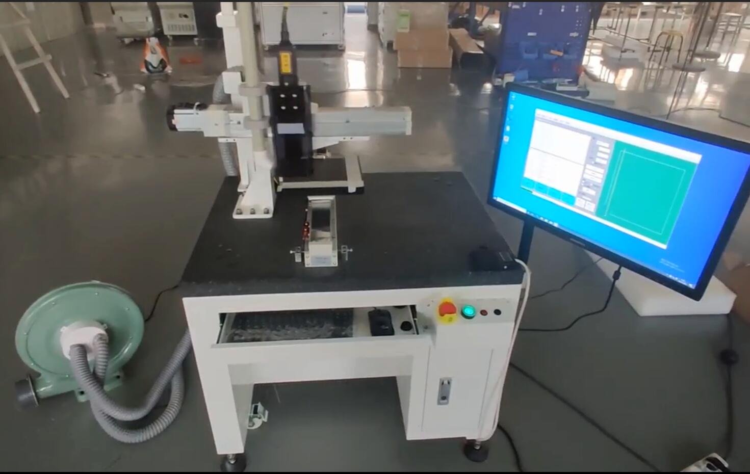
Solution Architecture: The Role of a Laser Scribing Machine
Advanced manufacturing solves these physical stress problems through non-contact precision. A high-quality Laser Scribing Machine completely isolates thermal and physical stress. It cuts the solar wafer without touching the material physically. This innovative approach ensures edge passivation remains completely intact. Intact passivation prevents electron recombination at the cell edges, keeping efficiency high.
Mitigating the Heat-Affected Zone (HAZ) remains the most critical function of this equipment. Laser ablation requires a delicate balance. The focused beam must remove material rapidly. However, it must also prevent thermal bleed from reaching the surrounding photovoltaic material. Keeping the HAZ practically nonexistent protects the cell's delicate electrical integrity. This balance enables the cell to capture weak, ambient light efficiently.
Beyond edge protection, laser systems provide unmatched geometric flexibility. Modern IoT casing designs increasingly demand irregular shapes. Smartwatches require circular cells. Automotive sensors need curved edge profiles. Programmable, software-driven cutting accommodates these irregular shapes effortlessly. You can adjust cutting paths instantly via CAD software. You no longer need to retool physical blades for different product runs.
We see clear, evidence-oriented results across the industry. Replacing mechanical saws with optimized laser scribing demonstrates undeniable benefits. Production lines typically report a verifiable reduction in micro-fracture incidents. Fewer micro-fractures correlate directly to significantly higher end-of-line yield metrics. Transitioning to non-contact tooling stops scrap at the source.
Key Evaluation Dimensions for a Laser Solar Cell Cutting Machine
Procurement teams must evaluate new equipment rigorously. You must map machine features directly to your expected production outcomes. A primary decision involves selecting the correct laser source.
Laser Source Type | Pulse Duration | Heat-Affected Zone (HAZ) | Ideal Material Application |
Nanosecond Laser | ~10⁻⁹ seconds | Moderate (Visible edge melting) | Standard Silicon IoT Cells |
Picosecond Laser | ~10⁻⊃1;⊃2; seconds | Minimal (Clean ablation) | Advanced Silicon, Thin-Film |
Femtosecond Laser | ~10⁻⊃1;⁵ seconds | Near-Zero (Cold ablation) | Perovskite, Highly Sensitive Layers |
Shorter pulse durations, like picosecond or femtosecond lasers, reduce HAZ dramatically. They provide "cold ablation" which evaporates material instantly. However, these shorter pulses increase your initial capital expenditure. You must align your laser type precisely to your specific cell architecture. Silicon, thin-film, and perovskite layers react differently to various wavelengths.
Beam positioning and optics represent another critical dimension. Galvanometer scanner precision dictates absolute edge smoothness. A high-end galvo scanner moves the laser beam rapidly and accurately. Smooth edges directly determine the micro-cell's long-term reliability in the field.
You must also evaluate scalability and Industry 4.0 integration. Evaluating a modern Laser Solar Cell Cutting Machine requires assessing its software backend. Can the machine interface smoothly with your existing Manufacturing Execution Systems (MES)? Look for robust Application Programming Interfaces (APIs). The system should offer real-time IoT connectivity. This allows predictive maintenance, automatic data logging, and remote vendor diagnostics.
Finally, understand the throughput versus edge quality trade-off. Many buyers focus entirely on top speed. Pushing a machine to its maximum millimeter-per-second transit speed often compromises edge integrity. High speeds can cause skipped pulses or increased thermal damage. You must base your evaluation on the optimal yield speed. Measure the speed at which the machine produces 100% acceptable parts, rather than its theoretical maximum velocity.
Implementation Realities, Risks, and Rollout Strategy
Integrating new laser technology into an existing facility presents logistical hurdles. You must assess integration bottlenecks early in the project lifecycle.
Footprint Constraints: Measure your available floor space carefully. Laser systems often require external chillers and power cabinets.
Utility Requirements: Assess your facility's cooling capacity. High-power laser diodes generate significant heat. You also need dedicated exhaust extraction for silicon dust.
Automation Handshakes: Review your material handling automation. Your vacuum loaders and unloaders must match the pace of your new scribing line seamlessly.
Operator capability is another major risk factor. Laser systems require highly specialized optical calibration. They also demand strict, daily maintenance routines. Your current operators will face a steep learning curve. We strongly advise securing comprehensive vendor training programs. Your maintenance team must learn how to clean protective lenses and align optics safely.
Compliance and safety remain non-negotiable. Verify all CE and FDA laser safety standards before purchasing. Ensure the equipment features true Class 1 safety enclosures. These enclosures protect operators from stray radiation. Check particulate extraction compliance. Vaporized silicon creates microscopic dust. You must filter this dust properly to protect your facility's air quality and worker health.
Validate all vendor assumptions thoroughly. Beware of vendor throughput claims based on simple, straight-line cuts. Real-world IoT cell cutting involves highly complex geometries, sharp corners, and circular paths. These intricate shapes force the laser scanner to accelerate and decelerate constantly. This movement dramatically lowers your actual Units Per Hour (UPH). Never plan your production capacity based on straight-line speeds.
Shortlisting Logic: Next Steps for Procurement and Engineering
How should procurement teams proceed? Choosing the right vendor requires a highly structured, evidence-based approach. Follow these logical steps to ensure equipment viability.
Step 1: The Proof of Concept (PoC). Never purchase industrial equipment purely based on spec sheets or marketing brochures. Demand a physical sample run. Provide the vendor with your exact cell materials. Give them your most complex required geometries. Evaluate how their machine handles your specific product.
Step 2: Third-Party Metrology. Do not rely solely on visual inspections. Independently verify the PoC samples using advanced metrology. Use electroluminescence (EL) imaging to spot dark areas. Apply scanning electron microscopy (SEM) to check for invisible, subsurface micro-cracks. These tests reveal the true edge quality.
Step 3: SLA and Support Infrastructure. Evaluate the vendor’s mean time to repair (MTTR) guarantees. Laser optics and diodes occasionally fail. Confirm local spare parts availability for critical components. International shipping delays for a replacement galvo scanner will halt your production line for weeks. Ensure the vendor has field service engineers in your region.
Step 4: Yield Rate Projections. Build a five-year production model. Compare the initial capital expenditure against consumable costs. Factor in lenses, specialized extraction filters, and energy consumption. Most importantly, calculate the projected scrap reduction value. A machine preventing just a 3% scrap rate often pays for itself rapidly in material savings alone.
Thorough evaluation prevents costly manufacturing delays. Follow this logic to secure equipment providing true operational excellence.
Conclusion
The decentralized power source remains a crucial bottleneck in the rapidly expanding IoT era. You cannot scale connected device production without highly reliable, miniature power supplies. High-yield production of custom micro-solar cells provides a distinct, measurable competitive advantage. Legacy mechanical cutting simply cannot support the precision or volumes required today.
Transitioning to advanced laser scribing offers more than a simple equipment upgrade. It represents a fundamental shift in your manufacturing capabilities. You move away from high-scrap, low-efficiency processes. You move toward high-margin, high-reliability component manufacturing. Non-contact cutting protects cell integrity, guarantees shape flexibility, and stabilizes production yields.
Take action on your production line today. Document your specific geometric shapes and minimum yield requirements. Contact your shortlisted equipment vendors immediately. Request customized sample testing using your proprietary silicon wafers. Evaluate the results through third-party imaging, and upgrade your facility to handle the next generation of IoT energy demands.
FAQ
Q: How does a laser scribing machine prevent efficiency loss in micro-solar cells?
A: It utilizes non-contact ablation using extremely short laser pulses. This precise method minimizes the Heat-Affected Zone (HAZ) along the cut perimeter. By isolating thermal and physical stress, it prevents microscopic fissures from forming in the silicon. Eliminating these cracks prevents electron recombination losses at the cell edges, preserving overall power output and efficiency.
Q: What is the typical ROI timeline for a commercial Laser Solar Cell Cutting Machine?
A: Your exact ROI timeline depends heavily on your production volume and current scrap rates. Financial models generally show a return on investment within 18 to 36 months. This rapid return is driven primarily by substantial raw material savings. You also gain increased revenue from achieving significantly higher tier-1 product yields compared to mechanical dicing.
Q: Can laser scribing systems handle next-generation thin-film or perovskite cells for IoT?
A: Yes, they absolutely can. However, processing these advanced materials requires specific wavelength and pulse-duration configurations. Manufacturers must use UV or ultrashort pulse lasers (femtosecond) to cleanly ablate the sensitive layers. This extreme precision prevents thermal damage to the underlying substrate. Vendor Proof of Concept testing remains mandatory for these advanced materials.
Q: What are the primary maintenance costs associated with this equipment?
A: Key operational expenses center around a few core hardware components. You must budget for regular protective optics replacement and scanner lens cleaning. Cooling system maintenance also requires scheduled fluid flushes. Finally, expect eventual laser diode degradation over tens of thousands of operational hours, requiring periodic refurbishment to maintain optimal cutting speeds.


