Photovoltaic manufacturing has shifted rapidly in recent years. We now see half-cut cells, shingled modules, and custom IoT solar applications dominating the market. Maximizing module power output requires zero-damage wafer separation. Legacy mechanical or thermal cutting methods are now obsolete. They simply cannot keep up. Older equipment crushes or melts modern, ultra-thin silicon wafers.
This article objectively evaluates advanced laser separation technology. You will learn how upgrading your equipment impacts production yield. We explore how it addresses complex integration risks on the factory floor. We also define the strict criteria you need for equipment selection. By understanding these dynamics, you can optimize your high-efficiency module production line. You can reduce waste, improve cell conversion rates, and future-proof your facility against evolving solar architectures.
Key Takeaways
Advanced laser separation minimizes the Heat-Affected Zone (HAZ), directly preventing micro-cracks and preserving long-term cell efficiency.
Implementing a high-throughput laser scribing machine enables the reliable production of half-cut cells, reducing module resistive losses.
Evaluating equipment requires moving beyond baseline cutting speeds to assess optical stability, automation integration, and real-world implementation downtime.
Proper integration reduces material waste but requires strict environmental controls and operator upskilling during the rollout phase.
The Yield Bottleneck: Why Legacy Cutting Limits High-Efficiency Modules
Traditional cutting techniques rely on harsh physical stress or immense heat. These methods worked fine for thicker legacy wafers. They fail miserably on modern high-efficiency architectures. You must understand these limitations to justify equipment upgrades.
The Cost of Micro-Cracks
Mechanical stress introduces microscopic defects along the cell edge. Outdated diamond wire or blunt thermal lasers create jagged margins. These microscopic faults seem harmless during initial factory sorting. However, field conditions expose them to severe thermal cycling. Sunlight heats the modules, and nightfall cools them. The silicon expands and contracts daily. Under these stresses, micro-cracks propagate inward. They eventually sever grid lines and create inactive dead zones. This leads to massive power degradation and costly warranty claims.
Efficiency Degradation and Edge Recombination
Heat damages silicon. Older thermal lasers literally melt the wafer to cut it. This aggressive process leaves behind a large Heat-Affected Zone (HAZ). A large HAZ alters the crystal lattice structure of the silicon. It introduces massive edge recombination losses. Electrons and holes recombine prematurely at the damaged edges instead of generating electrical current. This phenomenon directly lowers the final conversion efficiency of the cell. You lose precious wattage before the panel even leaves the factory.
The Automation Gap for Modern Wafers
Older equipment lacks modern optical precision. Manufacturers now produce ultra-thin silicon wafers to save material costs. Many top-tier wafers now sit below 130 micrometers in thickness. Mechanical cleaving systems struggle to handle these fragile components. They cause unacceptable breakage rates during high-speed inline processing. When a wafer shatters on the conveyor, it causes massive downtime. You must stop the line, clear the debris, and recalibrate. This automation gap ruins overall factory throughput.
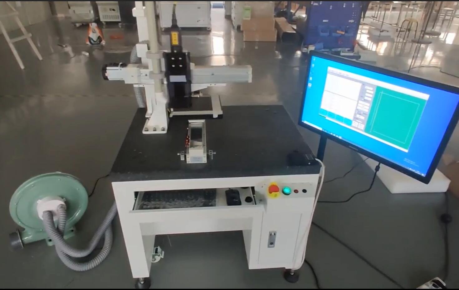
Core Mechanisms of a Modern Laser Scribing Machine
Upgrading your separation process requires specialized optical physics. You must implement a modern Laser Scribing Machine. These devices utilize advanced light manipulation to separate silicon without destroying it.
Non-Destructive Scribing (Cold Ablation)
Modern equipment relies on ultra-short pulse (USP) lasers. We categorize these as picosecond or femtosecond lasers. They operate at mind-boggling speeds. The laser pulse duration is shorter than the heat diffusion time of the silicon lattice. It vaporizes the material instantly. We call this process "cold ablation." The beam removes silicon without transferring damaging heat to the surrounding area. This physics breakthrough keeps the HAZ incredibly small, preserving cell integrity.
Precision Cleaving Process
Modern separation is not a brute-force cut. It is a highly controlled two-step process.
Precise Laser Grooving: The USP laser ablates a microscopic channel into the wafer surface. The depth usually reaches about one-third of the wafer thickness.
Controlled Splitting: The system applies mild mechanical bending or a secondary thermal stressor. This snaps the wafer perfectly along the grooved fault line.
This two-step method ensures incredibly smooth edges. Smooth edges resist mechanical stress much better than jagged ones.
Adaptability to Cell Architectures
Solar architectures change rapidly. Your factory might run PERC today and shift to TOPCon tomorrow. A high-quality laser system adapts easily. It handles diverse cell types without requiring complete optical overhauls.
PERC (Passivated Emitter and Rear Cell): Requires careful tuning to avoid damaging the delicate rear passivation layer.
TOPCon (Tunnel Oxide Passivated Contact): Demands precise energy control to protect ultra-thin tunnel oxide films.
HJT (Heterojunction Technology): Highly temperature-sensitive. HJT cells degrade rapidly above 200°C, making cold ablation absolutely mandatory.
Production Enhancements: From Half-Cut Cells to Custom IoT Modules
High-efficiency manufacturing relies on geometry. Changing the shape and size of the cell unlocks hidden power gains. You need the right machinery to execute these designs consistently.
Half-Cut Module Power Gains
Half-cut cell technology dominates the utility-scale market. The manufacturing logic is simple but powerful. When you split a standard cell in half, you reduce its electrical current by half. Physics dictates that resistive power loss equals the current squared multiplied by resistance (P = I⊃2;R). By halving the current, you cut the resistive power loss by a staggering 75%. This directly increases overall module output. It also lowers operating temperatures, which extends the module lifespan.
Throughput and Uptime Upgrades
Capacity upgrades must reflect realistic factory conditions. We measure this in wafers per hour (WPH). A modern Laser Solar Cell Cutting Machine comfortably processes upwards of 6,000 to 8,000 WPH. They achieve this through automated laser alignment systems. High-speed vision cameras constantly monitor the incoming wafers. They adjust the beam trajectory in milliseconds to account for slight positional shifts. This maintains continuous operation and eliminates micro-stoppages.
Customization for Emerging Markets
Solar energy now powers the Internet of Things (IoT). Sensors, smart home devices, and remote trackers require micro-solar panels. These applications demand custom, non-standard geometries. Modern laser software allows operators to program complex cutting patterns quickly. You can shift from standard half-cut production to custom hexagonal IoT cells in minutes. This flexibility opens lucrative new revenue streams for module manufacturers.
Production Output Comparison
Metric | Standard Full Cell | Half-Cut Cell Process |
Resistive Loss | Baseline (100%) | Reduced by 75% |
Shade Tolerance | Poor (entire string impacted) | High (bypass diodes isolate halves) |
Operating Temperature | Standard | Runs 2°C - 3°C cooler |
Micro-crack Risk | High (larger surface area) | Low (smaller footprint relieves stress) |
Evaluation Criteria for Equipment Selection
Choosing the right laser system dictates your factory yield for the next decade. Do not rely solely on advertised cutting speeds. You must dig deeper into optical stability and software architecture.
Optical System Stability
Consistent cut depth prevents wafer breakage. You must verify the beam quality using the M⊃2; factor. A perfect laser has an M⊃2; of 1.0. You should demand equipment testing below 1.2. Excellent pulse-to-pulse stability ensures every laser burst delivers the exact same energy. If the energy fluctuates, the groove depth varies. Shallow grooves cause irregular snapping. Deep grooves damage the underlying layers. Evaluate the laser source carefully before purchasing.
Automation and Industry 4.0 Integration
Hardware is only half the equation. You must evaluate the machine's software layer. Does it integrate seamlessly with your factory MES (Manufacturing Execution Systems)? Real-time yield tracking is mandatory. The machine must report edge chipping, breakage rates, and throughput metrics automatically. It should also feature predictive maintenance alerts. The system must notify technicians when optical lenses degrade, preventing unexpected downtime.
Vendor Compliance & Testing
Never buy equipment based on a brochure. You must enforce strict Factory Acceptance Testing (FAT). Standardized silicon behaves differently than your proprietary wafers.
Best Practices for FAT Execution:
Use Native Stock: Send your actual production wafers to the vendor facility for testing.
Microscopic Verification: Demand Scanning Electron Microscope (SEM) imaging of the cut edges to verify HAZ claims.
Mechanical Bend Tests: Perform 3-point bending tests on the cut cells. They must meet your minimum megapascal (MPa) fracture strength requirements.
Throughput Validation: Run the machine continuously for 8 hours. Verify it maintains advertised WPH without optical drift.
Implementation Realities and Rollout Risks
Installing highly sensitive optical equipment requires extensive preparation. Overlooking physical prerequisites will derail your production schedule and inflate costs.
Facility Requirements
Lasers despise vibrations and dust. You cannot simply bolt them to a standard factory floor.
Vibration Isolation: Nearby heavy machinery sends tremors through the floor. These tremors misalign the laser beam. You must install industrial-grade vibration isolation pads.
Climate Control: Temperature fluctuations alter optical lens behavior. Maintain strict, heavily regulated climate zones around the cutting station.
Exhaust and Filtration: Laser ablation generates toxic silicon dust. This dust coats lenses and ruins beam quality. Install specific localized exhaust systems with high-efficiency particulate air (HEPA) filtration.
Calibration and Commissioning Downtime
Set realistic expectations for your rollout. Integrating a new laser station into an existing high-speed line disrupts adjacent processes. The upstream conveyors must sync perfectly with the cutting station. Downstream sorters must adapt to new cell geometries. Green-field installations usually take two weeks to calibrate. Retrofitting existing lines often requires a month of weekend shutdowns to avoid halting current production completely.
Operator Training and Upskilling
Your maintenance crew must adapt. They are used to turning wrenches and aligning mechanical belts. Advanced laser systems require a completely different skill set. Operators must learn optical troubleshooting. They must understand software calibration, focal point adjustments, and lens cleaning protocols. Targeted upskilling is essential. Do not let untrained staff handle delicate optics, or they will cause expensive damage.
Common Mistakes in Implementation:
Failing to clean optics with specialized spectroscopic-grade solvents.
Ignoring ambient humidity, which fogs sensitive galvo mirrors.
Skipping daily beam profiling checks during the first month of operation.
Conclusion
Replacing mechanical stress with optical precision is mandatory for modern photovoltaic manufacturing. You cannot compete in the high-efficiency module market using outdated equipment. The transition to ultra-short pulse lasers virtually eliminates edge recombination and mechanical micro-cracks. This boosts your factory yield and secures your module warranties in the field.
When shortlisting equipment, look past the initial marketing specs. Prioritize vendors who offer transparent HAZ test data. Demand local integration support over those competing solely on price. The success of your rollout depends heavily on the vendor's willingness to tune the machine to your specific wafer architecture.
Action is required to stay competitive. Speak with your production engineers today. Instruct them to request a sample cutting test on your specific wafer material before initiating any procurement discussions. Real data will guide your best investment.
FAQ
Q: What is the acceptable Heat-Affected Zone (HAZ) for high-efficiency solar cells?
A: For modern high-efficiency cells like TOPCon and HJT, the acceptable HAZ must remain below 15 micrometers. Ultra-short pulse (USP) lasers operating in the picosecond or femtosecond range routinely achieve HAZ footprints of 5 to 10 micrometers. Keeping the HAZ this small prevents edge recombination losses and protects the cell's passivation layers.
Q: How does a laser scribing machine impact the mechanical strength of the cut cell?
A: A precise laser scribe creates a pristine, defect-free margin. Traditional cutting leaves microscopic jagged flaws that act as stress concentration points. By utilizing cold ablation and controlled splitting, the resulting edge is remarkably smooth. This drastically improves the cell's bending strength, making it highly resilient to thermal cycling and wind loads in the field.
Q: Can existing production lines be retrofitted with inline laser cutting stations?
A: Yes, existing lines can be retrofitted, but it presents synchronization challenges. The primary obstacle is matching the conveyor speeds between older equipment and the faster laser station. You must also account for the physical footprint and vibration isolation requirements. Retrofitting requires careful MES software integration to ensure upstream and downstream handoffs remain perfectly timed.
Q: What is the typical maintenance schedule for industrial laser cutting optics?
A: Industrial optics require strict daily and weekly maintenance. Operators must perform visual inspections and basic lens cleaning daily using approved spectroscopic solvents. Alignment checks and beam profiling usually occur weekly or bi-weekly. Core laser components, like the diode pump modules, typically offer a lifespan of 10,000 to 20,000 hours before requiring factory refurbishment or replacement.


