The shift toward half-cut and third-cut solar cells has completely redefined industry standards over the past few years. This evolution is especially evident when dealing with large wafer formats like M10 and G12. However, achieving perfect edge quality and preventing micro-cracks remain the primary bottlenecks in modern solar panel production lines.
Traditional mechanical cutting methods often fail to deliver the necessary precision for these fragile wafers. Standard thermal lasers introduce problematic heat-affected zones (HAZ) along the cut path. These thermal zones degrade overall cell efficiency and sharply increase unwanted breakage rates. Manufacturers clearly need a cleaner, more reliable approach.
For production managers and procurement engineers, investing in a specialized UV laser system demands careful evaluation. You must weigh upfront capital expenditure against substantial yield improvements and daily optical maintenance realities. This guide details exactly what you need to know. You will learn how cold ablation protects fragile silicon. We will also explore strict equipment criteria and actionable vendor evaluation metrics to help you optimize your high-volume production line.
Key Takeaways
Precision Over Speed: UV lasers utilize "cold ablation," significantly reducing HAZ and edge recombination losses compared to standard IR fiber lasers.
Yield Impact: Upgrading to a specialized laser solar cell cutting machine can drop cell breakage rates below 0.1%, directly improving production line ROI.
Format Scalability: Modern systems must natively support large wafer dimensions (156mm to 230mm) without requiring extensive mechanical retooling.
Total Cost of Ownership (TCO): While UV lasers offer superior precision, buyers must model for higher consumable costs (optical lenses/mirrors) and stricter environmental controls.
The Business Case: Why Production Lines Are Shifting to UV Lasers
Larger silicon wafers, specifically M10 and G12 formats, dominate modern panel manufacturing. They deliver higher module power output, but they present significant handling challenges. These large wafers are thinner and far more fragile than older generations. Conventional cutting methods rely heavily on thermal stress to separate the silicon. This intense, localized heat causes structural micro-cracks along the scribe line.
These microscopic fractures often remain completely hidden during initial factory inspections. They typically manifest later during module lamination. Worse, they can propagate during active field deployment due to wind or snow loads. This leads to catastrophic module failure and costly warranty claims.
Efficiency retention is another critical factor driving the shift to advanced technology. Mechanical scribing and high-heat lasers actively compromise the PN junction right at the cut edge. When thermal energy melts the silicon, the delicate dopant profile shifts. This damage leads to measurable power loss, known as edge recombination. We must eliminate this junction damage to maintain high wattage in half-cut cell configurations.
Here is a breakdown of common micro-crack sources in traditional cutting:
Excessive thermal gradients from infrared laser melting.
Mechanical stress from snapping wafers after a shallow scribe.
Vibrations transferred through poorly calibrated conveyor belts.
Inconsistent beam focus causing uneven thermal penetration.
Ultraviolet lasers offer a powerful, scientifically proven solution. Operating at a 355nm wavelength, they rely on photochemical ablation. They break molecular bonds directly rather than relying on photothermal melting. This mechanism is frequently called "cold ablation." It protects the fragile silicon structure and preserves the electrical characteristics of the edge.
When planning your facility upgrade, you should define clear, aggressive success criteria. First, target a drastically reduced breakage rate. A premium Laser Solar Cell Cutting Machine should easily push breakage rates below 0.1%. Second, demand absolute zero power degradation at the cut edge. Finally, ensure the new system maintains your required UPH (Units Per Hour) throughput without sacrificing precision.
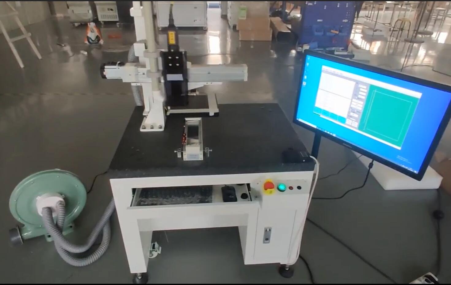
UV vs. IR Fiber Lasers in Solar Cell Scribing
Many facilities still debate between infrared and ultraviolet wavelengths for their production floors. The choice directly impacts production yields, maintenance schedules, and final module wattage. Let us examine the fundamental differences driving equipment selection today.
IR fiber lasers operate at a 1064nm wavelength. They offer high thermal penetration into silicon substrates. They generally provide faster absolute cutting speeds in straight lines. However, they carry a remarkably high risk of micro-cracks. They easily damage fragile silicon and specialized photovoltaic glass. The deep thermal penetration melts the material violently, causing splatter and thermal stress.
In contrast, UV lasers operate at 355nm. They feature shallow material penetration. Silicon absorbs UV light exceptionally well. This massive absorption rate means the energy breaks atomic bonds instantly before heat can spread. This results in incredibly clean, debris-free grooves.
Edge quality represents another critical differentiator. UV lasers produce a nearly negligible heat-affected zone. You eliminate the need for costly post-cut etching. Aggressive chemical cleaning baths become entirely unnecessary. IR lasers leave a prominent, damaged zone requiring extensive secondary processing.
Application fit depends entirely on your exact product mix. You should choose IR lasers for thick, non-critical structural cuts where edge aesthetics do not matter. Conversely, choose UV lasers for high-efficiency solar cell splitting. They excel at processing advanced architectures like PERC, HJT, and TOPCon cells. They also handle precision thin-film glass scribing flawlessly.
Feature | IR Fiber Lasers (1064nm) | UV Lasers (355nm) |
Ablation Method | Photothermal (Melting and Vaporization) | Photochemical (Direct Bond Breaking) |
Heat-Affected Zone (HAZ) | Large, frequently risks micro-cracks | Negligible, preserves cell efficiency |
Best Application Fit | Thick glass, structural non-active cuts | High-efficiency cells (PERC, HJT, TOPCon) |
Post-Cut Processing | Often requires chemical etching or cleaning | Clean groove, ready for immediate assembly |
Core Evaluation Criteria for a Laser Scribing Machine
Evaluating a high-end Laser Scribing Machine requires looking far beyond basic marketing brochures. You must align equipment capabilities with demanding daily factory realities.
First, rigorously evaluate throughput and scribing speed. Manufacturers often advertise extremely high maximum scribing speeds in millimeters per second. However, raw speed means nothing if cornering accuracy degrades. Always measure cutting speed against the Galvo scanner's stabilization time. If the mirrors vibrate slightly at high speeds, your scribe line will waver. Demand data on effective speed during continuous pattern tracing.
Second, verify wafer size compatibility. The solar industry constantly shifts toward larger form factors to boost module power. Your selected system must adapt quickly without requiring hours of mechanical downtime. We strongly recommend an adjustable staging system. It should natively handle dimensions ranging from 156mm up to 230mm wafers.
Third, examine the beam quality closely. Engineers use the M⊃2; factor to measure beam perfection. Look for an M⊃2; value as close to 1.0 as possible. A highly focused, perfect beam guarantees a very narrow kerf width. This saves valuable silicon real estate and increases the active generation area of the solar cell.
Fourth, prioritize robust automation and vision systems. Wafer warping is a daily challenge on the production floor. Your machine must include high-resolution CCD cameras. They enable dynamic optical alignment. They also use rapid fiducial recognition to compensate for physical warping instantly. If the printed busbars shift slightly from wafer to wafer, the vision system must adjust the scribe path in milliseconds.
Finally, demand a strict breakage rate guarantee from the manufacturer. Ask the vendor for specific SLA-backed metrics. They must define the maximum allowable breakage during continuous 24/7 operation. A machine that performs well during a five-minute demo might fail during a week-long stress test.
Implementation Risks and Maintenance Realities
Adopting ultraviolet technology introduces new operational dynamics to your facility. You must prepare your production team for specific maintenance realities. UV systems behave differently than standard infrared fiber systems.
Optical degradation happens significantly faster with ultraviolet light. Shorter wavelengths carry much higher photon energy. This intense energy is incredibly harsh on delicate optical coatings. You should expect shorter lifespans for Galvo mirrors. Focusing f-theta lenses will also degrade quicker compared to standard IR systems. If microscopic dust settles on a UV lens, the high-energy beam will instantly burn it into the coating. You must budget for scheduled, routine optical replacements to maintain beam quality.
Environmental sensitivity requires strict facility upgrades. UV laser resonators demand precise ambient controls. You must regulate temperature and humidity perfectly within the machine's enclosure. Factory environments must prevent any condensation on the optics. Fluctuating temperatures can misalign the internal resonator crystals, causing sudden power drops.
Debris management remains a high priority. While cold ablation is significantly cleaner than thermal melting, it is not perfectly clean. The photochemical process still generates sub-micron silicon dust. You must evaluate the machine's exhaust capabilities thoroughly. Ensure it features robust integrated downdraft extraction. High-efficiency HEPA filtration systems are absolutely mandatory to keep the internal optics clean.
Consider your current operator skill levels. Calibrating UV pulse durations requires specific expertise. Tuning repetition frequency settings demands specialized training. Assess the vendor’s software interface during your evaluation. It should facilitate easy, intuitive recipe management. A well-designed software interface reduces the learning curve for your technicians and prevents costly setup errors.
Shortlisting Vendors and Next-Step Actions
Selecting the right vendor dictates your long-term production success. Never purchase a complex laser system based on specification sheets alone. You must take systematic, verifiable steps to prove equipment performance before signing a contract.
Begin with a comprehensive Proof of Concept (PoC). Send your specific silicon wafers directly to the vendor's application lab. If you cut specialized PV glass, send those samples as well. Demand a custom sample cut using your exact CAD files and speed requirements.
Next, perform rigorous microscopic verification on the returned samples. Do not rely solely on basic visual inspections. Post-sample, utilize Scanning Electron Microscopy (SEM). Combine this with Electroluminescence (EL) imaging. These diagnostic tools definitively verify the absolute absence of hidden micro-cracks. They also prove the heat-affected zone is truly negligible.
Then, confirm the system's integration capability. Check the exact machine footprint to ensure it fits your existing factory layout. Validate all factory communication protocols. SECS/GEM and MES compatibility are non-negotiable for modern smart factories. They guarantee seamless data integration into automated solar module assembly lines.
Evaluate the vendor's service and support infrastructure. Determine their regional footprint. They must stock critical spare parts locally. Pay special attention to laser diode and f-theta lens availability. Demand guaranteed technician response times to minimize costly production downtime.
Actionable Vendor Evaluation Steps
Request a dedicated Proof of Concept using your actual M10 or G12 wafer stock.
Conduct independent SEM and EL imaging on the provided samples to check for hidden defects.
Audit the vendor's software for seamless MES integration compatibility.
Review the regional service contract for guaranteed part availability and response times.
Conclusion
Integrating a sophisticated UV laser system represents a highly strategic manufacturing upgrade. You must balance strict facility maintenance and regular optical care against unmatched cutting quality. The resulting cell efficiency retention fundamentally transforms your production output. UV cold ablation protects your extremely fragile M10 and G12 wafers from thermal stress.
Prioritize vendors who transparently discuss optical consumable lifespans rather than hiding them. They should enthusiastically prove their breakage rate claims through rigorous testing. Demand volume-based sample testing on your exact cell formats to verify UPH metrics. By focusing on advanced precision processing, you secure higher yields, lower scrap rates, and deliver superior, reliable solar modules to the global market.
FAQ
Q: Can a UV laser scribing machine cut both silicon solar cells and photovoltaic glass?
A: Yes, it can process both materials, but it requires completely different pulse settings and power outputs. UV light is excellent for surface scribing thin-film glass. However, ultra-fast lasers, such as picosecond or femtosecond models, are sometimes preferred for thick structural glass cutting. They effectively prevent shattering on thicker substrates.
Q: What is the typical kerf width achieved with a UV laser solar cell cutting machine?
A: Depending on the beam quality and focusing optics, kerf widths typically range from 15μm to 30μm. This extremely narrow cut minimizes valuable material waste. It maximizes the active generation area of the solar cell, directly contributing to higher overall module efficiency.
Q: How does cell size (e.g., 156mm vs. 230mm) affect the laser cutting process?
A: Larger cells require a significantly larger working field from the Galvo scanner. Alternatively, they need highly precise XY-stage indexing. Scribing larger cells dramatically increases the risk of thermal bowing. This makes the precise cold ablation of a UV laser absolutely critical for large M10 and G12 formats.
Q: What is the typical lifespan of the UV laser source before requiring a major overhaul?
A: High-quality solid-state UV laser sources typically operate reliably for 15,000 to 20,000 hours. After this period, a significant drop in power output usually necessitates diode replacement or factory refurbishment. Keep in mind that external optical lenses and mirrors require much more frequent maintenance.


